

Electrical and Electronic Engineering
Devices and Systems for Information
Electronic Devices
Kansei Nano-Biosensor Research Laboratory
 Members : Assoc.Prof. Takeshi Onodera
keywords : Taste sensor, Odor sensor, Foods, Biomarker, Sensing
We are researching and developing sensors for taste and odor sensing.
– Odor and gas sensing using inverse opal photonic crystals
– Further functionalization of taste sensors developed through science and technology that combines biotechnology and electronics
– Development of biosensors targeting small molecules in body fluids such as blood, urine, sweat, and saliva, as well as those derived from plants
– Development of sensors that surpass the dog nose in detecting odorants such as explosives and fragrances with ultra-high sensitivity using antigen-antibody reactions.
Based on these studies, we are also conducting research to try to apply and deploy these technologies in various fields.
Integrated magnetic device laboratory
 Members : Assoc.Prof. Terumitsu Tanaka
Our laboratory focus on the study of novel magnetic phenomena and the development of magnetic devices forming three dimensional fine structures using nanometer sized microfabrication technologies. The numerical and experimental advanced researches are being implemented for realizing future ultra-high density recording devices such as hard disk drives and magnetic random access memories, and novel functional logic devices.
Plasma Engineering Laboratory
 Members : Prof. Masaharu Shiratani / Prof. Kazunori Koga / Assoc.Prof. Kunihiro Kamataki / Assoc.Prof. Takamasa Okumura
Plasma Engineering Laboratory (PEL) is nationally and internationally renowned for our research regarding plasma science. Principal research challenges in PEL are as follows:
- Development of high quality and high throughput processes by controlling reactions in plasma,
- Plasma synthesis of functional nanoblocks and their application,
- Elucidation of interaction between plasma and interface of materials,
- Establish of plasma agriculture.
Present research topics are as follows:
- Development of novel solar cells,
- Third generation solar cells using nanoparticles,
- Deposition profile control in fine structure using anisotropic plasma chemical vapor deposition,
- Nanoparticle composite films for ultra low-k film in ULSI,
- Fabrication of nanosystems using plasmas,
- Mechanism of dust particle formation and transport in fusion devices,
- Plasma growth enhancement of plants.
Spintronic Device Laboratory
 Members : Prof. Hiromi Yuasa / Asst.Prof. Yuichiro Kurokawa
keywords : Spin of electron, Nano magnetic film, Data memory & storage, thermoelectric device
In spintronics, in addition to the charge of electrons, which plays a major role in electronics, the rotation of electrons, or “spin,” plays an important role. Spin mainly appears in magnetic materials that are attracted to magnets, so we conduct research using magnetic materials. Using spin could lead to green devices with no electron flow and zero Joule loss, and even to power generation using waste heat. The answer to the future of electronic devices has yet to be found. We are challenging ourselves to create a better society through spintronics research.
Electronic Materials & Devices Laboratory
 Members : Prof. Naho Itagaki / Assoc.Prof. Tamiko Oshima
keywords : sputtering, oxide semiconductor, zinc oxide, crystal growth, heteroepitaxy, inverse SK mode, In2O3:Sn, amorphous transparent conducting oxides
An exciton, which is an electrically neutral quasiparticle, is a bound state of an electron-hole pair attracted by the electrostatic Coulomb force. The most interesting feature of an exciton is that it can be generated by and converted back into a photon within a short time (<nsec). Thus, excitonic devices potentially bring great improvements to the speed of electronic–optical (E/O) conversion along with significant miniaturizations of E/O converters. The major challenges for excitonic devices are finite exciton binding energy (Eex) and finite exciton lifetime. The small exciton binding energy of typical excitonic materials, such as GaAs, limits the device operation temperature below 125K. While, the exciton lifetime in such materials is less than a nanosecond, allowing excitons to travel only a small distance before it recombines. In this laboratory, we have developed an excitonic device with a new semiconducting material, (ZnO)x(InN)1-x (abbreviated as ZION), which has large Eex as well as large piezoelectric constant. The large Eex potentially enables excitonic devices that are operational at room temperature. Another advantage is the long exciton lifetime, allowing excitons to travel long distance before it recombines. The aforementioned excellent properties of ZION films and its QWs open a new avenue for studies toward the practical use of excitonic devices.
Constructive Electronics Laboratory
 Members : Assoc.Prof. Takeaki Yajima
keywords : Semiconductor, Oxide thin film, Phase transition, Low-power circuits, Recurrent neural network
The 21st century is the age of information. However, as information technology accelerates, the hardware that supports it will consume infinite amount of power and communication bandwidth. A completely new hardware technology is required to create a sustainable society for the next 100 years. The operating principles of biological neural circuits are now attracting attention as a potential source of such technology. Their resilience and energy-saving properties, which have been refined through long evolution, are exactly what is required to build a sustainable society. In our laboratory, we are extracting useful technologies from neural circuits and applying them to the next generation of information processing hardware. We utilize highly versatile circuit technology and material technology to create a variety of functions.
Computer System Architecture Laboratory
 Members : Assoc.Prof. Satoshi Kawakami
keywords : Computer Architecture, Circuit design, Optical Computing, Superconducting Single Flux Quantum Computing, Machine Learning, Neuromorphic
Processors, the core of our information processing society, are reaching their limits in terms of high performance and low power consumption. On the other hand, advanced and complex applications such as big data and AI processing are exploding in popularity. In particular, we aim to realize dedicated computers for AI applications using innovative devices (optical/superconducting). We are also working on the invention of a “zero-energy” computer that overturns the conventional wisdom of computers. In collaboration with researchers from inside and outside the university, you will acquire cutting-edge knowledge across each technical layer (algorithm, architecture, circuit, and device), so those who are intersted in pioneering innovative computing are welcome to join.
Quantum Device Engineering Laboratory
 Members : Assoc.Prof. Haruki Kiyama
keywords : Semiconductor, Quantum Device, Nanotechnology, Quantum Computer, Spin, Quantum Information, Nanofabrication, Cryogenic Technology
In Quantum Device Engineering Laboratory, we study quantum transport phenomena in semiconductor quantum structures such as quantum dots. We fabricate nanometer-scale quantum devices using state-of-the-art technologies, and measure its transport properties at extremely low temperatures (typically below one Kelvin). Furthermore, single electron spins in quantum dots are promising candidates of qubits for quantum computers. We also study spin manipulation, spin readout and other fundamental technologies for large-scale integration of spin qubits.
Bioinspired Microsystems Laboratory
 Members : Assoc.Prof. Fumihiro Sassa
keywords : Micro-robots, BioMEMS, kinetic electronics, Biochemical sensors, Cell manipulation and culture microdevices
We conducts exploratory research on bio compatible manufacturing technologies and micro-device applications, using microfabrication techniques for various materials, including biological tissues, as well as Bio-MEMS (Bio MicroElectroMechanical Systems) as core technique. The remarkable advancements in medicine and life sciences in this century are expected to lead to large-scale direct manipulation at the cellular level and comprehensive treatment of individual cells. A promising approach to achieving this is the mass fabrication of micro-robotic structures through microfabrication. However, current Si-based MEMS devices are prone to damage when exposed to liquids or friction due to their rigid structure. So, We are working on the development of “biocompatible, flexible, and highly durable integrated micro-robot fabrication techniques” that inspired from flexibility of biological organs. We are also developing devices that enable high-density cell culture on chips and self-healing functional elements, based on microfabrication technique of various materials.
Semiconductor Spintronics Laboratory
Members : Assoc.Prof. Naoto Yamashita
Keywords : spintronics, semiconductor, spin current, reactive sputtering, magnetic thin film
Rooted in fundamental physics and driven by the goal of creating innovative devices, our research focuses on the field of spintronics from three key perspectives: crystal growth, interfacial physics, and device physics. The core of our research lies in spin currents—the flow of spin angular momentum. We are particularly passionate about understanding and advancing their generation, transport, and control, as these processes form the foundation of innovative spintronic technologies.
Currently, we are working in the following three specific areas in spintronics:
– Spin current transport in semiconducting materials
– Spin orbital torque in ferrimagnetic insulators
– Spin-caloritronic device
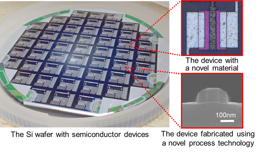
Atomic Layer Process Laboratory
Members : Prof. Hiroki KONDO
Keywords : Semiconductor integrated circuits (ULSI), 3D nanotransistors, atomic layer process (ALP), plasma process, reliability physics
Do you know how many and what type of transistors are in your smartphone? The conventional metal/oxide/silicon (MOS) structure found in textbooks no longer exists, and smartphones are equipped with more than 20 billion transistors with a few nanometer scales (about the same wideth as the double helix of DNA). To realize future electronics that will become even more miniaturized and highly integrated and will be integrated with quantum computers, we are researching the science of thin film and surface reactions at the atomic layer order and the dynamics of nanodevice degradation (reliability physics).
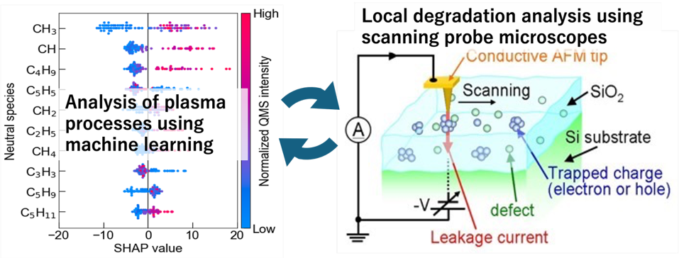
1. Plasma-Excited Atomic Layer Process Science
We quantitatively interpret the non-equilibrium reaction field between the active species generated in plasma and the wafer using informatics such as machine learning, leading to innovation in materials and processes.
2. Device Reliability Physics
~Visualization of material and structural degradation at the atomic layer~
We use scanning probe microscopes and transmission electron microscopes to observe the degradation inside nanoscale devices at the atomic level in real time, and elucidate its mechanism.
Integrated Electronics
Radio-Frequency Integrated Circuits (RFIC) & Microwave Communication Device Laboratory
 Members : Prof. Haruichi Kanaya
Cooperating chair : Prof. Kuniaki Yoshitomi
keywords : IoT, Radio wireless communication, CMOS circuit, Antenna, Implant, Endoscope, Energy harvesting circuit, Power amplifier
In this laboratory, we are now focusing our researches on the following areas:
- High speed, high linearity and low noise system LSI components for wireless communications systems.
- Wideband RF front-end components for ultra-wideband (UWB) applications.
- Digital Radio or Digital RF Processor and its system components i.e. Digitally assisted RF/Analog circuits such as ADPLL (All-digital phase locked loop), DCO (digitally-controlled oscillators), sampling mixers, digital controlled PA and LNA etc. for Software defined radio or other reconfigurable applications.
- Electrically small antennas for narrow band and UWB applications.
- Interconnection and packaging technology of a chip to an antenna to reduce parasitic components.
- RF micro energy harvesting circuit for medical application
Microdevice Laboratory
 Members : Assoc.Prof. Ryo Takigawa
keywords : semiconductor, transistor, integrated circuit, three-dimensional integrated circuit, image sensor, terahertz, SiC, power device
The transistor possesses the function that controls the output current by the input voltage. This simple function has been producing tremendous impact on the human society. For example, there are billions of transistors in a computer to memorize and process information. Information communication is also realized by using the function of transistor. On the other hand, transistors enable us to sense physical information in the real space which we live. Thus transistors provide driving force to create infrastructure for human life in the era of Society 5.0 where cyber-physical space technology is designed for humanity.
The Microdevice Laboratory caries out research on semiconductor transistors. We are anxious to create new function with the transistor physics. We are also interested in processing technology to produce transistors. One of our research subject is to produce imaging devices which can extract information using invisible light or radio waves. The other research interest is to produce high efficiency power controlling devices which will contribute to sustainable growth of the society.
Information Photonics Laboratory
 Members : Assoc.Prof. Naoya Tate
keywords : Optical computing, Optical security, Optical neural network, Nanophotonics, Quantum dot engineering
“Information photonics” refers to a broad class of computing-related technologies that utilize light as an information carrier, and that are established through the integration of photonic and information technologies to enable a wide range of operations in physical space, including information generation, acquisition, transmission, storage, retrieval, and presentation. In this context, we particularly adopt the concept of “Photonics × Nanotechnology × Information” as our guiding principle. Based on advanced knowledge and experimental techniques for the functional design and construction of microscopic physical systems ranging from the micrometer to nanometer scale, we are engaged in the development of innovative optical computing devices and systems that operate at the macroscopic scale.
Micro / Nano Laser Device Laboratory
 Members : Prof. Yuji Oki / Asst.Prof. Yuya Mikami
keywords : Silicone Optical Technology (SoT), Optical organic materials, Optical waveguides, Semiconductor lasers, Optoelectronic devices, 3D printer
We are conducting research on XXX. In the Micro/Nano Laser Device Group, we conduct research in the fields of laser engineering and organic optoelectronics. Our research primarily focuses on the development of printable photonic devices, including organic lasers and photodetectors based on micro- and nanostructures utilizing organic materials. In addition, we are engaged in research on semiconductor lasers, diode-pumped solid-state lasers, and ultraviolet-light-based organic material processing. We are also pursuing advanced measurement technologies utilizing these optical technologies.
Furthermore, in the field of communications, we aim to achieve fundamental solutions to the challenges faced by modern society through the creation and demonstration of novel optoelectronic devices and photonic-electronic integrated systems. By integrating state-of-the-art photonic and electronic technologies, our research seeks to develop new concepts in optoelectronics and advanced integrated systems for future information and communication technologies.
Semiconductor Devices Integration Laboratory
 Members : Assoc.Prof. Hisashi Kino
Keywords : Semiconductor device, Integrated circuit, Semiconductor package
Integrated circuit technologies are important for supporting the current information society from a hardware side, and their importance is growing year by year. Our group aims to improve the performances of integrated circuits by incorporating new structures and materials into semiconductor devices. For instance, we are researching ways to improve the performance of semiconductor devices by incorporating special materials that shrink when heated and expand when cooled.
We are also researching ways to develop new application fields for semiconductor technology, such as medical and sensor devices.
Students study these topics through design and fabrication themselves.
Cyclic Integrated Photonics Laboratory
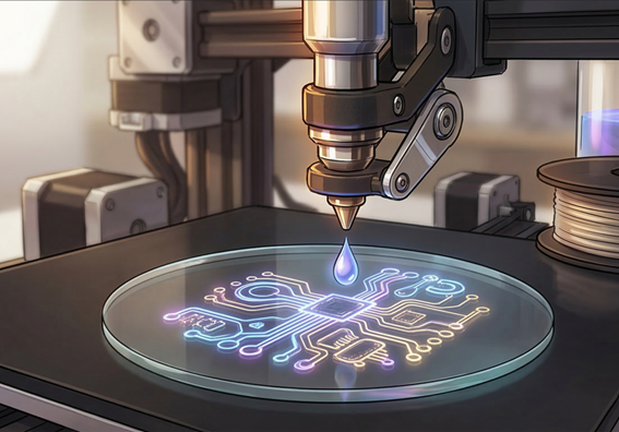 Members : Assoc.Prof. Hiroaki Yoshioka / Asst.Prof. Jinghan Chen
keywords : Quantum photonic integrated circuits, Table-top Fabrication, Lasers, Structured light, Organic optical materials, Ephemeral Photonics
“Optical chips” support our smartphones and the global internet. Currently, they are manufactured in massive factories and discarded after use. We are challenging this norm by developing “Table-top Fabrication,” a technology to print and integrate optical circuits on demand using a desktop printer. Furthermore, we are pioneering “Ephemeral Photonics”—a new, eco-friendly lifecycle for optical devices where circuits are born from liquid ink, function dynamically through molecular circulation, and naturally degrade or are reconfigured after their role is complete.
Devices and Systems for Energy
Measurement and Control Engineering
Superconductivity Laboratory
 Members : Prof. Takanobu Kiss / Assoc.Prof. Kohei Higashikawa / Asst.Prof. Zeyu Wu
keywords : Superconductivity, Critical current properties, Advanced measurement technology, Electrical and electronic materials, Power and energy applications, Advanced medical system
Our studies focus on understanding and resolving key performance issues of forefront superconducting materials and their power applications. We have been developing high performance superconducting materials which can carry high current more than 100 of times larger than that of conventional copper conductors with almost no dissipation. Perspectives of these studies are to lead breakthrough to such fields as power grid, alternative energy, transportation and advanced medical systems. We educate young researchers, graduate-, and under-graduate-students through the research projects in collaboration with national- and international counter parts.
Mathematical Systems Theory Laboratory
 Members : Prof. Yoshio Ebihara
keywords : Dynamical systems, Control systems theory, Optimization theory, AI and machine learning
In this laboratory we conduct analysis and synthesis of dynamical systems using control systems theory and optimization theory. In particular, recently we focus on algorithms and neural networks used in AI and machine learning fields and try to establish their reliability and stability from rigorous mathematical point of view. We promote these studies in close collaboration with the members from LAAS-CNRS, Toulouse, France.
Applied Energy Engineering
Control & Optimization Laboratory
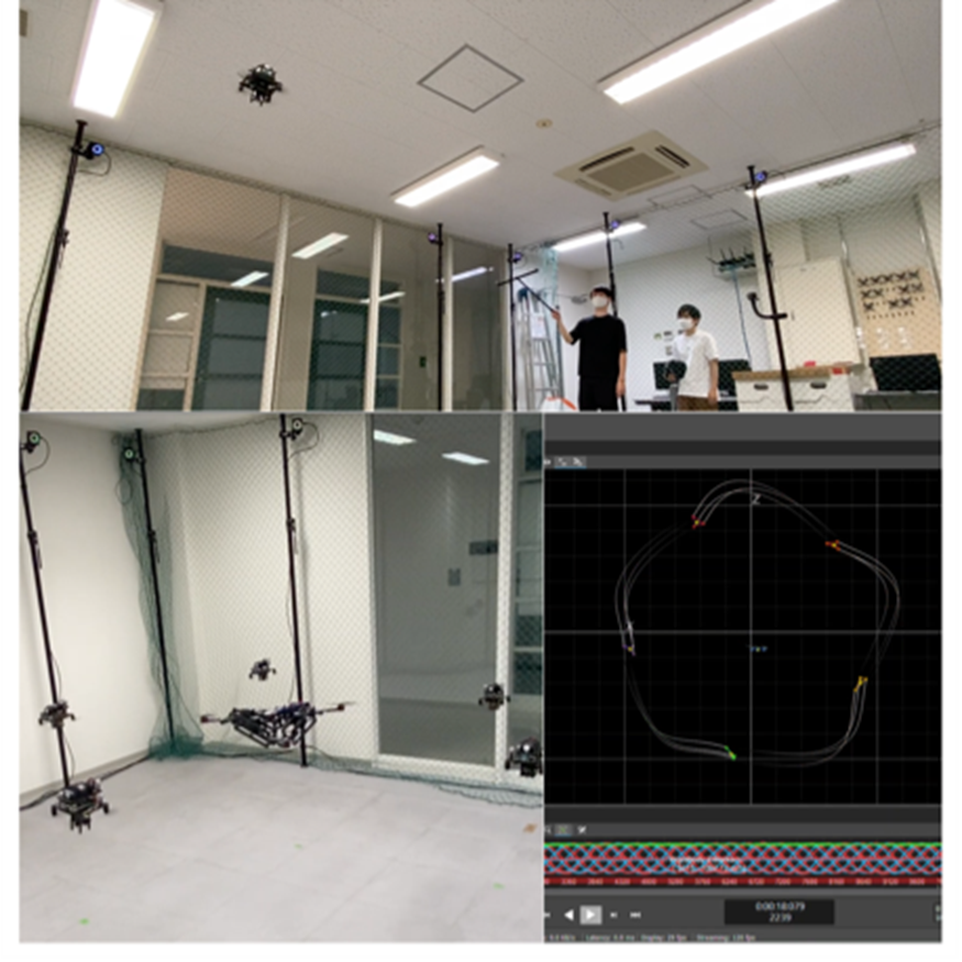
Members : Assoc.Prof. Kaoru Yamamoto / Assoc.Prof. Andreas Themelis / Asst.Prof. Akinori Sakaguchi
keywords : Multi-robot/drone control, flocking control, sampled-data
Our lab conducts research using control theory to make robots, drones and other systems move as intended. In particular, we focus on the control of autonomous mobile robot fleets, such as platooning of self-driving vehicles and coordinated flight of multiple drones. Each robot makes decisions based on local information, and we study how to control the whole system so that it moves in a stable and efficient manner. We are also developing advanced methods in sampled data control theory, which is essential for improving the accuracy and stability of computer-based control systems. This area plays a key role in cyber-physical systems, which combine physical and virtual worlds. In addition, we are working not only on the application of optimization algorithms to path planning and control design, but also on their theoretical foundations. We are also developing transformable drones that can operate in confined or complex environments, with the aim of performing tasks such as collecting data from disaster sites that conventional drones cannot.
Inorganic Functional Materials x Excimer Laser Laboratory
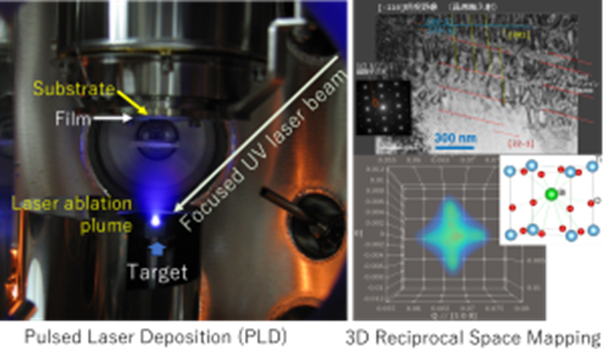
Members : Prof. Hisato Yabuta
keywords : Inorganic semiconductors, ferroelectric materials, oxide superconductors, excimer-laser annealing, pulsed lased deposition
Today’s electronic devices use not only traditional materials, such as silicon for semiconductors, but also many newly discovered materials with functions that were previously unknown. For example, oxide materials like glass are used in smartphones and tablet PCs as semiconductors for transistors instead of silicon. Our research is focused on finding new inorganic materials, adding new functions and properties to them, and forming these as thin films to be used in modern devices. For this research, we use excimer lasers, which generate powerful ultraviolet beams, to synthesize new materials and process them to produce new functions.We are studying to make sure that these new materials and functions will be used in the next generation of devices.
Applied Electromagnetic Energy Laboratory
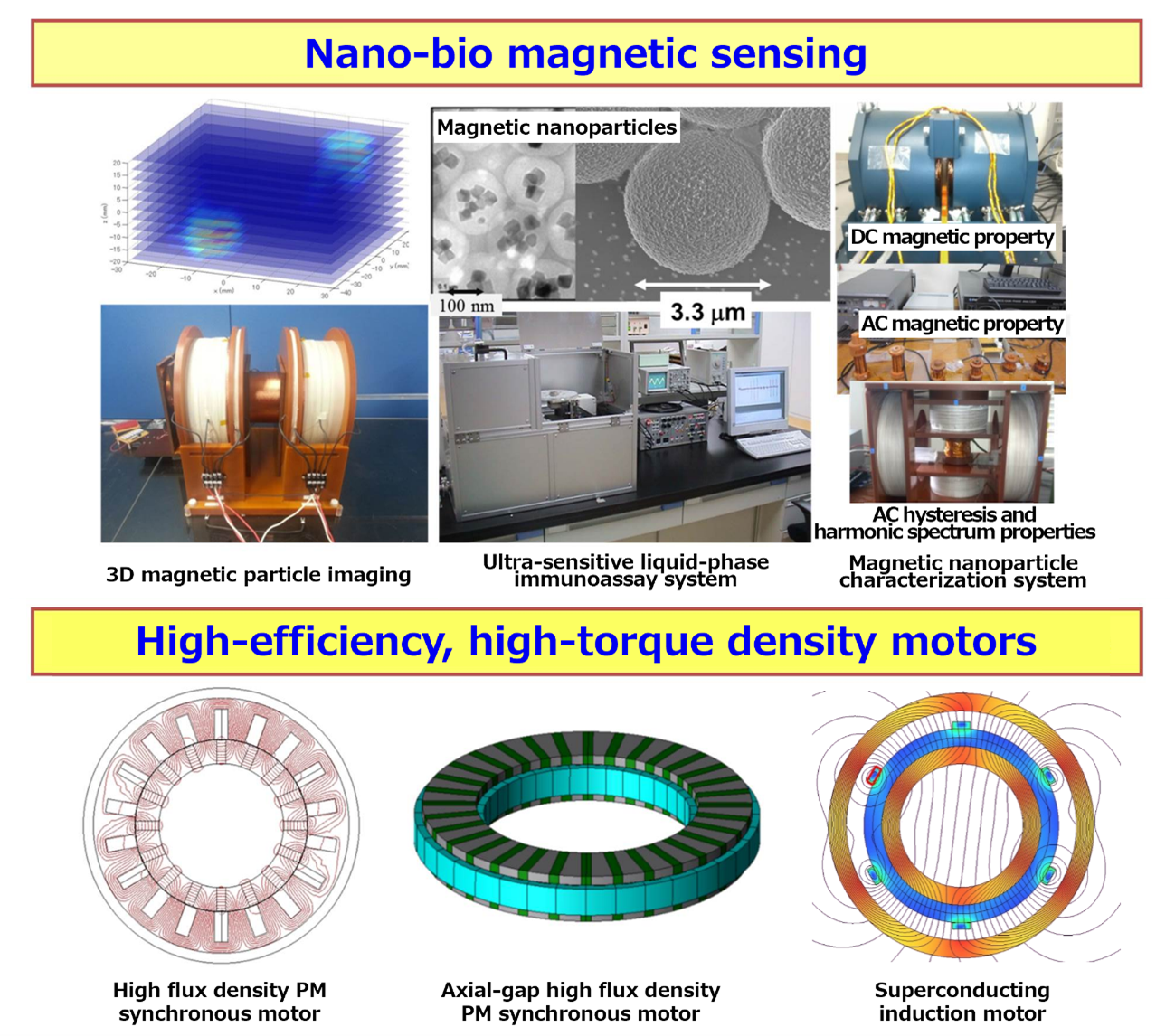
Members : Prof. Takashi Yoshida / Asst.Prof. Hiromasa sasa
keywords : Magnetic nanoparticles, Magnetic particle imaging, High output power density motor, Superconducting motor
We are developing novel medical systems and high-performance electrical machines based on “magnetism”. “Magnetism” enables the contactless transfer of force and energy, and the contactless detection of magnetic signals without being affected by the human body. Devices that take advantage of these unique properties in “magnetism” are widely utilized in both medical and industrial fields. Our research in medical applications focuses on rapid and highly sensitive sensing and imaging technologies using magnetic nanoparticles. Additionally, we are developing high-performance electrical machines, such as superconducting motors, for applications in electric aircraft and other applications.
Superconductive Systems Engineering
Laboratory of Advanced Magnetic Sensing System
 Members : Assoc.Prof. Teruyoshi Sasayama
We can obtain information inside a specimen in a non-contact and non-destructive manner by using a magnetic field. By utilizing this advantage, advanced magnetic sensing devices with unprecedented high performance and new functions can be developed, which are applied to a wide range of fields such as medical and biotechnology, analysis and evaluation, and environmental measurement. In our laboratory, we are developing ultrasensitive magnetic sensors for detecting weak magnetic fields, and are aiming to apply these magnetic sensors to medical devices and nondestructive testing. Specifically, in medical devices, we are developing a magnetic imaging device for cancer using magnetic markers. In nondestructive testing, we are developing devices to inspect defects inside various structures used in social infrastructure.